NVIDIA has yet to dispatch their whole Pascal representation card lineup and gossipy tidbits have as of now began indicating at their up and coming GPU design. Reported more than years prior, the Volta GPU was to be NVIDIA's next most prominent chip architectur to supplant Maxwell yet was pushed back with Pascal having its spot. With Pascal improvement finish, NVIDIA has set their endeavors in the building up their most recent GPU extend.
NVIDIA Volta Architecture Rumored To Be Featured in High-Performance GV102, GV104 and GV110 GPUs
The gossip on NVIDIA Volta GPU comes straight from the Motley Fool who could acquire some huge subtle elements on the cutting edge chip architecture through a Chinese source. As per the talk, NVIDIA is preparing a scope of chips that will use the Volta architecture. Not just that, the Volta GPU architecture has been fundamentally redone and will offer a genuine change regarding execution and power productivity contrasted with the Pascal GPUs.
The site notices improvement of three GPUs in view of the Volta design is in progress. The previous evening, NVIDIA affirmed amid their income get that they have taped out and completed improvement for all Pascal GPUs however they will present every one of them at different time allotments. This announcement affirms that NVIDIA's advancement office is currently centered around completing Volta in time. In any case, I might want to call attention to that advancement on these GPUs had started much before as it took NVIDIA three years to build up the Pascal design with an aggregate cost between 2-3 billion dollars.
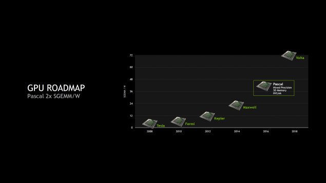 Volta GPUs would feature a huge leap in performance per watt compared to current gen chips.
The gushing multiprocessor obstruct for Pascal and Maxwell was comparative yet was incomprehensibly tuned alongside the move up to the new FinFET hub which prompted to some great increments. Volta then again will highlight a totally new outline no matter how you look at it.

NVIDIA Volta Architecture Rumored To Be Featured in High-Performance GV102, GV104 and GV110 GPUs
The gossip on NVIDIA Volta GPU comes straight from the Motley Fool who could acquire some huge subtle elements on the cutting edge chip architecture through a Chinese source. As per the talk, NVIDIA is preparing a scope of chips that will use the Volta architecture. Not just that, the Volta GPU architecture has been fundamentally redone and will offer a genuine change regarding execution and power productivity contrasted with the Pascal GPUs.
The site notices improvement of three GPUs in view of the Volta design is in progress. The previous evening, NVIDIA affirmed amid their income get that they have taped out and completed improvement for all Pascal GPUs however they will present every one of them at different time allotments. This announcement affirms that NVIDIA's advancement office is currently centered around completing Volta in time. In any case, I might want to call attention to that advancement on these GPUs had started much before as it took NVIDIA three years to build up the Pascal design with an aggregate cost between 2-3 billion dollars.
following are the chips that are rumored to be introduce as high-end gaming GPUs:
- NVIDIA GV110 GPU
- NVIDIA GV102 GPU
- NVIDIA GV104 GPU
Volta has long been part of NVIDIA’s roadmap and there’s no doubt that most of the work on these chips will be nearing competition as we enter 2017. During these phase, engineering secrets leak out and we are looking at a similar situation where someone was hinted about Volta’s architecture enhancements. According to the rumor, Volta is significantly redesigned compared to the Pascal architecture.
NVIDIA’s Pascal architecture has significant gains in almost all departments over Maxwell but it’s also fact that Pascal and Maxwell share a common DNA. The SM design for both chips is very same. Aside from the GP100 GPU which is different due to its FP64 hardware blocks, the GP106, GP104 and GP102 share a lot in common with Maxwell designs.
NVIDIA Maxwell (GM204) and Pascal (GP104) SM Designs:
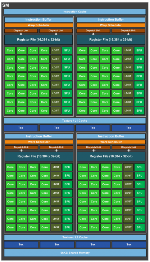


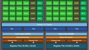
The gushing multiprocessor obstruct for Pascal and Maxwell was comparative yet was incomprehensibly tuned alongside the move up to the new FinFET hub which prompted to some great increments. Volta then again will highlight a totally new outline no matter how you look at it.
NVIDIA GV102, GV104 For High-End Gamers, GV110 Also Aimed at Consumer Market?
Starting with the GV104 GPU, we know from the name that this chip will replace the GP104 GPU and will be the most ideal chip for gamers with a decent price tag. NVIDIA’s most successful cards came from the G*104 series of GPUs since the Fermi series. Moving on, we can see vastly improved performance from such chips. The next chip in the stack is GV102. Succeeding the GP102 which is housed inside the GeForce GTX Titan X (P) card, the new high-performance chip will be aimed at enthusiasts who demand serious horsepower.
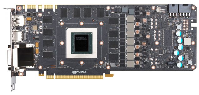
The Titan X features the high-end GP102 chip with insane amounts of horse power.
The third chip is the most fascinating as it is likewise specified as a gaming chip. Known as GV110, the GPU will be a definitive outline highlighting the Volta design. As of now, the GP100 GPU is the bigon top of Pascal line and is housed inside the HPC accelerators , for example, Tesla P100. This chip is worked for twofold accuracy workloads and outlined around NVLINK interconnect
The GP100 GPU is also the only chip that utilizes the fastest HBM2 memory. Now GV110 is interesting as it recalls the naming scheme of GK110. GK110 was also a chip which featured the double precision capabilities, however they were cut down on the consumer variants.
NVIDIA Volta will be featured inside two (100+ PFLOPs) supercomputers.
With GP102 and GP100, NVIDIA has tried to maintain parity in terms of performance while getting rid of the non-essential features that are not required in gaming and professional workloads (FP64/NVLINK). GV110 can be the full fat chip with limited FP64 capabilities designed for the prosumer market.
It will be interesting to see how this works out but we shouldn’t expect Volta GPUs this soon. The closest we will hear anything official from NVIDIA on Volta would be their GTC
GPU Family
|
AMD Vega
|
AMD Navi
|
NVIDIA Pascal
|
NVIDIA Volta
|
Flagship GPU
|
Vega 10
|
Navi 10?
|
NVIDIA GP100
|
NVIDIA GV110
|
GPU Process
|
FinFET
|
7nm FinFET?
|
TSMC 16nm FinFET
|
FinFET
|
GPU Transistors
|
15-18 Billion
|
TBC
|
15.3 Billion
|
TBD
|
Memory (Consumer Cards)
|
HBM2?
|
Next-Gen Memory
|
GDDR5X/HBM2
|
GDDR5X/HBM2?
|
Memory (Dual-Chip Professional/ HPC)
|
HBM2
|
Next-Gen Memory
|
HBM2
|
HBM2
|
HBM2 Bandwidth
|
512 GB/s (Instinct MI25)
|
>1 TB/s?
|
732 GB/s (Peak)
|
1 TB/s (Peak)
|
Graphics Architecture
|
Next Compute Unit (Vega)
|
Next Compute Unit (Navi)
|
5th Gen Pascal CUDA
|
6th Gen Volta CUDA
|
Successor of (GPU)
|
Radeon RX 500 Series?
|
Radeon RX 600 Series?
|
GM200 (Maxwell)
|
GV110 (Volta)
|
Launch
|
2017
|
2018
|
2016
|
2017-2018
|